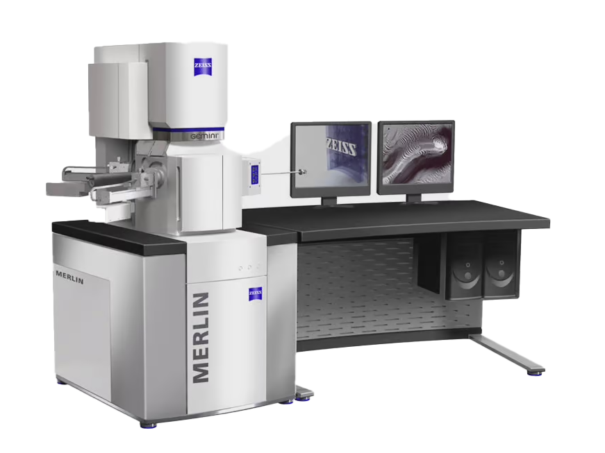
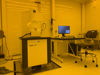
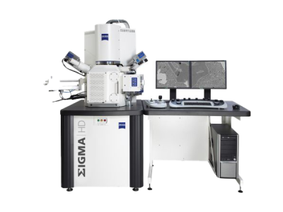
Zeiss Merlin high-resolution scanning electron microscope is a versatile electron beam characterization tool for semiconductor research, life and material sciences. It is capable of high resolution secondary electron imaging with a resolution of 0.8 nm at 15KV and 1.4 nm at 1 kV with in-lens secondary electron detector. It is also equipped with a retractable 4 Quads and an in-lens energy selective backscatter detectors for back-scattered electron imaging, an unique charge compensation system for imaging of non-conductive materials, and a scanning transmission electron microscopy (STEM) detector for studying of electron-transparent thin film samples. A software to reconstruct 3D surface topography is also available. Accessories include an EDS for X-ray microanalysis and elemental mapping and an EBSD for crystallographic texture study.
- Magnification: x12-2M
- Acceleration: Voltage 0.02-30kV
- Probe current: 3pA-40nA
- 5-axes motorized eucentric specimen stage (X,Y=130mm, Z=50mm, T=-4deg-70deg, R-360deg)
Detectors
- Everhart Thornley Secondary Electron Detector
- Inlens Secondary Electron Detector
- Inlens Energy Selective Backscatteres Electron Detector (EsB)
- Angular selective Backscattered Detector
- Annular STEM Detector (aSTEM4)
- EDS Detector
- EBSD
Please make sure to acknowledge MIT.nano Characterization in any publication, presentations, and patents involving results originated from the use of the Gemini 450 SEM at MIT.nano Characterization Focus Facilities or through assistance from MIT.nano staff.
Suggested language: "This work was performed in part in the MIT.nano Characterization Facilities"
Anna Osherov, PhD
12-5005
Connor Moorman
12-0184
James M. Daley
39-421
Zhenyuan Zhang
13-1025

Only qualified users can reserve and use the instrument. The reservations are limited to 4 hr instrument time.
13-1025
MIT.nano (basement level)
60 Vassar Street (rear)
Cambridge, MA


